
Scientists at the University of Wisconsin’s Materials Research Science and Engineering Center (MRSEC) on Nanostructures, Materials, and Interfaces have demonstrated a technique that could one day allow electronic devices to assemble themselves automatically – giving semiconductor manufacturers a way to mass-produce “nanochips” that have circuit elements only a few molecules across, roughly ten times smaller than the features in current-generation chips.
“In terms of storage alone, that could mean a computer with 4,000 gigabytes of memory,” says center director Juan de Pablo, a member of the Wisconsin team, which is publishing its results in the journal Nature.
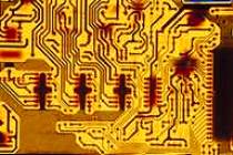
In today’s chip fabrication plants, solid-state circuit elements are etched onto the surface of a wafer of silicon via lithography: a process that’s somewhat like exposing photographic film and then developing it. That approach has gotten the manufacturers down to features on a scale of 100-150 nanometers, which is typical of current-generation chips like the Pentium 4. “But the cost of the factories is increasing at an exponential rate,” says de Pablo, “and it’s not clear if they can extrapolate their current technology much below 50 nanometers.”
Some experimental techniques can go smaller. For example, a tightly focused electron beam can inscribe nanoscale circuit elements on the silicon surface line by line, almost as if an artist were drawing them with a pen. The problem is that drawing a single chip takes something like a week. With lithography, which can imprint a pattern on the entire wafer surface at once, the big fabrication plants can mass-produce thousands of chips in an hour.
Another technique getting attention works from the bottom up, using materials that will spontaneously assemble themselves into periodic structures at the molecular scale. “Achieving dimensions of tens of nanometers is inexpensive and routine,” says Nealey – especially with certain “block copolymers,” which are compounds composed of two or more long polymer chains connected at the ends, like so: �AAAAAAA�BBBBBBB�CCCCC� Unfortunately, he says, left to their own devices, these materials tend to organize themselves into roundish clumps and broad, swirling patterns, nothing like the precisely ordered structures needed for technological applications.
Next, Nealey and his colleagues washed the patterned silicon surface with a solution containing the block copolymer. In this case, it was a compound containing just two types of component polymers: one that had a chemical attraction to the stripes, and another that preferred to stay out in the open air. By manipulating the length of the two polymers, and other such factors, the researchers achieved a very precise balance between attraction and repulsion. And as a result, the co-polymer organized itself right on top of the nanoscale stripes, with no evidence of swirling or other undirected behavior.
Of course, de Pablo cautions, it’s a long way from parallel lines of plastic to fully operational electronic devices. “All that we’ve done in this work,” he says, “is to create the pattern, show that the polymer follows the pattern, and show that the final result is completely free of defects.” Nonetheless, Nealey points out, this work is a proof of principle: “We’ve shown that this kind of hybrid technology can integrate self-assembling materials, such as block copolymers, into existing manufacturing processes, such as lithography, and deliver molecular level control.”
The next step may be to grow the block copolymer in nanoscale vertical columns, says Nealey. Such columns eventually could be engineered to hold one bit of information each, leading to ultra-high density magnetic storage media – probably “the most immediate and striking application” of the hybrid technology, he says. A more speculative application would be to create nanoscale integrated circuits. After all, says Nealey, many polymers can be made to conduct electricity if they contain the right kind of metal ions. So in principle, one could dope different parts of the polymer pattern with different ions, and make devices such as diodes and transistors.
The tricky part would be designing the circuits themselves. “The industry has been using the same integrated circuit designs for years,” says Nealey, “just shrinking them as the chips get smaller. But here we can’t do that; with our technique we can only make very simple shapes like lines and circles. On the other hand, if we can make these simple designs very inexpensively, then the question for the chip designers becomes, ‘What can we do with this?'”
“That’s a huge unknown,” says Nealey. “But it will be a big research area in the future.”


Comments are closed.